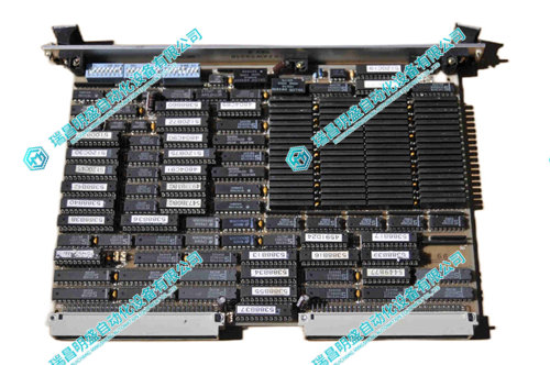
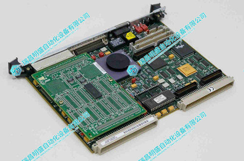
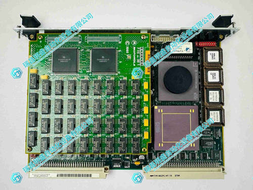
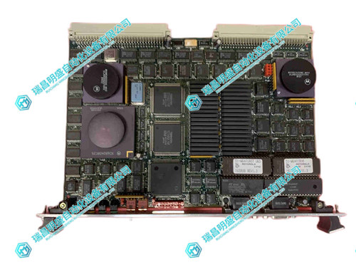
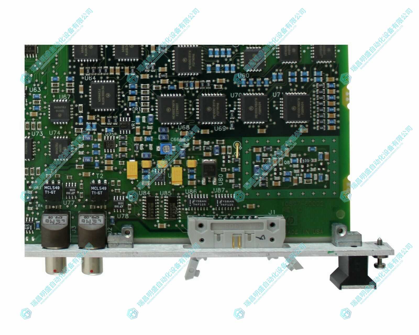
Nikon 45007-691-1 印制板
产品详情:
印制电路板(Printed Circuit Board,PCB)是一种用于支持和连接电子元件的基础组件,广泛用于各种电子设备和系统中。它是一块薄而坚固的板,上面印刷有导电路径,用于连接和支持各种电子元件,如电子元件、集成电路、连接器和其他组件。以下是关于印制电路板的一些关键信息:
用途:PCB 用于在电子设备和系统中提供电路连接和支持。它可以是各种设备的核心部分,如计算机、手机、电视、工业控制系统、医疗设备等。
导电路径:PCB 上的导电路径通常由导电材料(通常是铜)印刷在绝缘基材(通常是玻璃纤维强化树脂)上。这些导电路径形成了电路,允许电流在电子元件之间流动。
层次结构:PCB 通常具有多层结构,其中多个印刷的层叠在一起,每一层都包含导电路径和绝缘层。多层 PCB 允许更复杂的电路设计。
元件安装:电子元件通常通过焊接或插入方式固定在 PCB 上。这些元件可以是表面安装元件(SMT)或插件式元件。
设计和制造:PCB 的设计通常使用计算机辅助设计(CAD)工具进行,然后通过印刷技术制造。制造 PCB 包括印刷、蚀刻、钻孔、焊接、覆盖层制造等过程。
定制设计:PCB 可以根据具体应用的需求进行定制设计。不同的应用可能需要不同形状、尺寸、层数和特定电路布局的 PCB。
应用领域:PCB 广泛应用于电子工业中,包括通信设备、消费电子、工业自动化、医疗设备、航空航天等领域。
刚性和柔性 PCB:刚性 PCB 通常用于要求结构稳定性的应用,而柔性 PCB 可以弯曲和卷起,适用于空间有限的场景。
实物拍摄图片:

product details:
Printed Circuit Board (PCB) is a fundamental component used to support and connect electronic components, widely used in various electronic devices and systems. It is a thin and sturdy board printed with conductive paths for connecting and supporting various electronic components, such as electronic components, integrated circuits, connectors, and other components. Here are some key information about printed circuit boards:
Purpose: PCB is used to provide circuit connections and support in electronic devices and systems. It can be the core part of various devices, such as computers, mobile phones, televisions, industrial control systems, medical equipment, etc.
Conductive path: The conductive path on a PCB is usually printed on an insulating substrate (usually glass fiber reinforced resin) using a conductive material (usually copper). These conductive paths form circuits that allow current to flow between electronic components.
Hierarchy: PCB usually has a multi-layer structure, where multiple printed layers are stacked together, each layer containing conductive paths and insulation layers. Multilayer PCBs allow for more complex circuit designs.
Component installation: Electronic components are usually fixed to the PCB by welding or inserting. These components can be surface mounted components (SMTs) or plug-in components.
Design and manufacturing: PCB design is usually carried out using computer-aided design (CAD) tools, which are then manufactured through printing technology. Manufacturing PCBs includes processes such as printing, etching, drilling, welding, and overlay manufacturing.
Customized design: PCB can be customized according to specific application requirements. Different applications may require PCBs of different shapes, sizes, layers, and specific circuit layouts.
Application field: PCB is widely used in the electronic industry, including communication equipment, consumer electronics, industrial automation, medical equipment, aerospace and other fields.
Rigid and flexible PCBs: Rigid PCBs are typically used in applications that require structural stability, while flexible PCBs can be bent and rolled up, suitable for scenarios with limited space.
相关站内产品推荐:
-------------------------------------------------本篇文章来自瑞昌明盛自动化设备有限公司https://www.mingshengplc.com/


