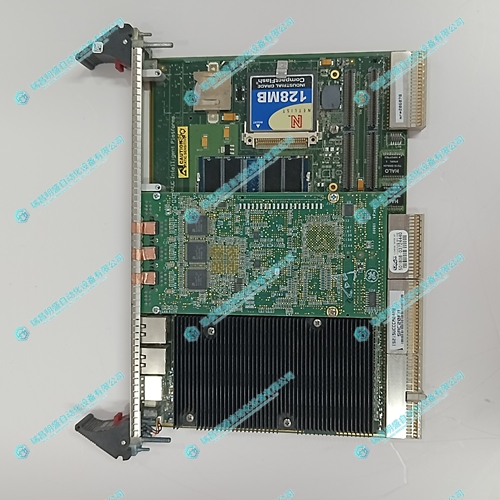
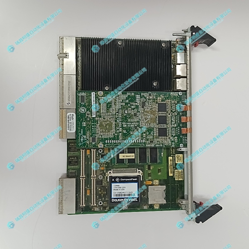


NIKON 4S020-090 印刷电路板
产品详情:
印刷电路板(Printed Circuit Board,PCB)是一种用于支持和连接电子元件的基础电子部件。PCB通常由绝缘性的基板材料(通常是玻璃纤维增强的环氧树脂,也称为FR-4)制成,上面覆盖着导电性的铜箔层,通过化学腐蚀或机械方式制作电路。以下是关于印刷电路板的一些重要信息:
导电路径:PCB上的铜箔层被设计成形成导电路径,以连接各种电子元件,例如电阻、电容、晶体管、集成电路等。这些导电路径通常被称为"导线"或"线路",它们将电流从一个元件传输到另一个元件。
孔洞:PCB上通常有孔洞,用于安装和连接元件。这些孔洞可以通过插入元件引脚并焊接来实现连接。它们还可以用于连接不同PCB层之间的导线。
印刷标记:PCB通常具有印刷标记,这些标记包括元件的引脚编号、电路图符号、元件值、元件位置等信息。这些标记有助于装配和维护过程中的可识别性。
层数:PCB可以是单层、双层或多层的。多层PCB包含内部层,通常用于提供电源平面和地平面以降低电磁干扰(EMI)和提高信号完整性。
连接器:连接器或连接线通常用于将PCB连接到其他电子设备或系统。它们提供了电源、数据和信号的接口。
设计软件:PCB的设计通常使用专门的PCB设计软件,工程师可以在其中绘制电路图、布局元件、设计导线和生成制造文件。
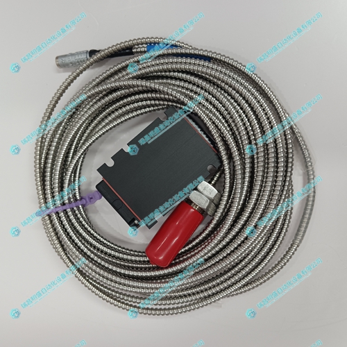
实物拍摄图片:

product details:
Printed Circuit Board (PCB) is a basic electronic component used to support and connect electronic components. PCB is usually made of insulating substrate material (usually glass fiber reinforced epoxy resin, also known as FR-4), covered with a conductive copper foil layer, and circuits are made through chemical corrosion or mechanical means. Here are some important information about printed circuit boards:
Conductive path: The copper foil layer on a PCB is designed to form a conductive path to connect various electronic components, such as resistors, capacitors, transistors, integrated circuits, etc. These conductive paths are commonly referred to as "wires" or "lines", which transmit current from one component to another.
Holes: PCBs usually have holes for installing and connecting components. These holes can be connected by inserting component pins and welding. They can also be used to connect wires between different PCB layers.
Printed markings: PCBs typically have printed markings, which include information such as component pin numbers, circuit diagram symbols, component values, and component positions. These markings contribute to the identifiability during assembly and maintenance processes.
Number of layers: PCB can be single layer, double layer, or multi-layer. Multilayer PCBs contain internal layers, typically used to provide power and ground planes to reduce electromagnetic interference (EMI) and improve signal integrity.
Connector: A connector or connecting wire is usually used to connect a PCB to other electronic devices or systems. They provide interfaces for power, data, and signals.
Design software: PCB design usually uses specialized PCB design software, where engineers can draw circuit diagrams, layout components, design wires, and generate manufacturing files.
相关站内产品推荐:
-------------------------------------------------本篇文章来自瑞昌明盛自动化设备有限公司https://www.mingshengplc.com/