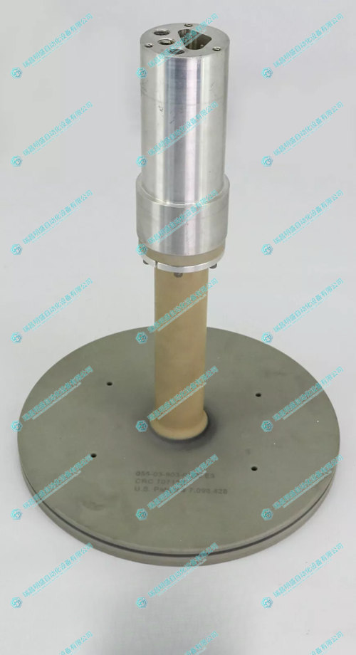
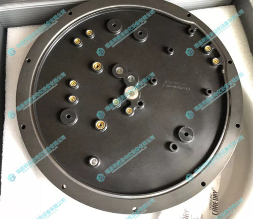


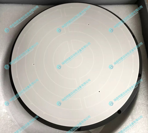
LAM 839-019090-611静电夹
1.产 品 资 料 介 绍:
中文资料:
LAM 839-019090-611 是一款用于半导体制造设备的静电夹(Electrostatic Chuck, ESC),主要用于在晶圆加工过程中固定和控温。以下是其特点和应用领域:
主要特点:
静电吸附
利用静电力牢固固定晶圆,避免机械夹持造成的损伤。
精确控温
内置加热和冷却系统,实现晶圆温度的精确控制。
高可靠性
设计适用于高真空和等离子体环境,具有长寿命和稳定性能。
多种尺寸兼容
支持不同尺寸的晶圆(如 200mm、300mm),适应多种工艺需求。
低污染
采用高纯度材料制造,减少对晶圆的污染。
快速响应
温度调节响应速度快,适合高精度工艺要求。
易于集成
设计符合半导体设备标准,便于安装和维护。
应用领域:
半导体制造
用于刻蚀、化学气相沉积(CVD)、物理气相沉积(PVD)等工艺。
平板显示制造
在液晶显示器(LCD)和有机发光二极管(OLED)生产中用于薄膜沉积和刻蚀。
太阳能电池制造
用于光伏电池的薄膜沉积和表面处理。
光学镀膜
用于光学镜片和滤光片的镀膜工艺。
科研与实验室
支持材料科学和半导体工艺的研究。
总结:
LAM 839-019090-611 静电夹是一款高精度、高可靠性的晶圆固定和控温设备,广泛应用于半导体制造、平板显示制造、太阳能电池制造、光学镀膜和科研领域,满足高精度工艺的需求。
英文资料:
LAM 839-019090-611 is an electrostatic chuck (ESC) used in semiconductor manufacturing equipment, mainly for fixing and temperature control during wafer processing. The following are its characteristics and application areas:
Main features:
Electrostatic adsorption
Use electrostatic force to firmly fix the wafer and avoid damage caused by mechanical clamping.
Accurate temperature control
Built in heating and cooling system for precise control of wafer temperature.
high reliability
Designed for high vacuum and plasma environments, with long lifespan and stable performance.
Compatible with multiple sizes
Supports wafers of different sizes (such as 200mm, 300mm) to meet various process requirements.
Low Pollution
Made with high-purity materials to reduce wafer contamination.
quick response
Fast temperature regulation response speed, suitable for high-precision process requirements.
Easy to integrate
Design in accordance with semiconductor equipment standards for easy installation and maintenance.
Application areas:
Semiconductor Manufacturing
Used for processes such as etching, chemical vapor deposition (CVD), physical vapor deposition (PVD), etc.
Flat panel display manufacturing
Used for thin film deposition and etching in the production of liquid crystal displays (LCDs) and organic light-emitting diodes (OLEDs).
Manufacturing of solar cells
Used for thin film deposition and surface treatment of photovoltaic cells.
Optical Coating
Coating process for optical lenses and filters.
Research and Laboratory
Support research in materials science and semiconductor processes.
Summary:
LAM 839-019090-611 electrostatic clamp is a high-precision and highly reliable wafer fixing and temperature control device, widely used in semiconductor manufacturing, flat panel display manufacturing, solar cell manufacturing, optical coating, and scientific research fields, meeting the needs of high-precision processes.
2.产 品 展 示
3.其他产品
4.其他英文产品
A-B 1794-IRT8XT Relay Output Module
Teknic SST-1500-XCX Digital Servo Drive
| PMB31B-00114-03 | AMAT 0100-18039 | PFRL101D 5.0KN 3BSE002969R0002 |
| PMB31B-00114-02 | IMDSO02 | 3BUR980025R1 DSTX 180 |
| PMB31B-00114-01 | 70 AS 41b-E | N32HREM-LNK-NS-00 |
| PMB31B-00114-00 | 07AB67R1 | P21NRLC-LSS-NS-03 |
| PMB31B-00101-03 | ICFC16l1 | N31HRLJ-LNK-NS-01 |
| PMB31B-00101-02 | AMAT 0100-20234 | 57160001-PE DSDI 126 |
| PMB31B-00101-01 | IEPAF02 | 57160001-BH DSTD 110 |
| PMB31B-00101-00 | AMAT 0100-90554 | PFTL201C 20.0KN |
| PMB31B-00100-00 | NKTU116 | M21NSXC-LNN-NS-02 |