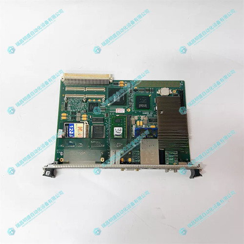
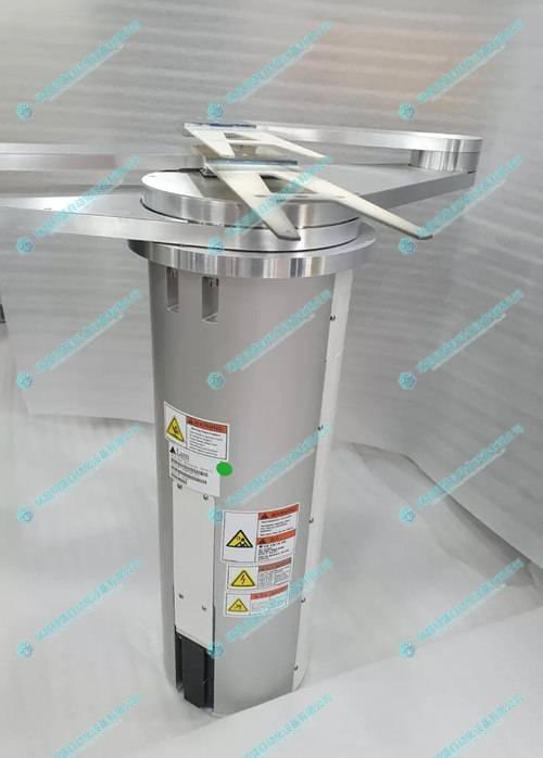
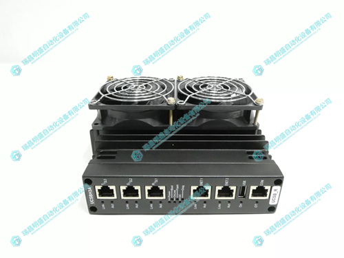
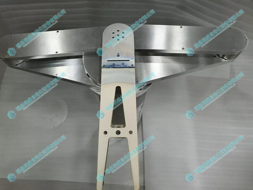


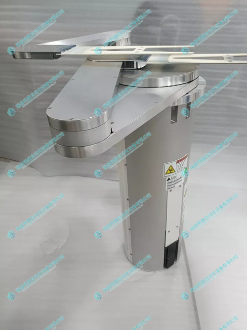
LAM 853-227247-001机器人套装
1.产 品 资 料 介 绍:
中文资料:
LAM 853-227247-001 机器人套装 主要用于 半导体制造 领域,特别是在 晶圆加工 过程中,实现 精确、高效的自动化晶圆传输。它是 Lam Research 设备中的重要组件,适用于 前道(Front-End)和后道(Back-End)工艺,确保生产过程的高精度和高可靠性。
产品应用领域
半导体制造(晶圆处理)
- 光刻(Lithography):在光刻工艺中,需将晶圆精准送入光刻机并取出,确保对准和无损传输。
- 刻蚀(Etching):用于等离子刻蚀(如 Lam Research 9400, TCP 9600, Versys 等设备),精准传输晶圆,避免颗粒污染。
- 沉积(Deposition):适用于 化学气相沉积(CVD)、原子层沉积(ALD)、物理气相沉积(PVD) 设备,确保均匀处理。
- 离子注入(Ion Implantation):将晶圆从传输系统送入离子注入机,确保精准对准,提高工艺控制能力。
- 清洗(Cleaning):配合清洗设备(如 SPTS Omega 系列),安全处理超薄晶圆,防止破损。
面板显示(FPD,Flat Panel Display)
- 适用于 OLED、LCD、MicroLED 面板制造,保证大尺寸玻璃基板的精准传输,防止划痕和微尘污染。
先进封装(Advanced Packaging)
- 在 2.5D、3D IC 封装 过程中,用于晶圆级封装(WLP)、倒装芯片(Flip-Chip)等生产线的自动化搬运。
其他高精度自动化
- 光通信、MEMS、功率半导体制造:支持高精度芯片传输,适用于 SiC、GaN 等材料的特殊工艺。
- 实验室自动化:用于科研设备,提供精确的样品搬运方案。
英文资料:
The LAM 853-227247-001 robot kit is mainly used in the semiconductor manufacturing field, especially in wafer processing, to achieve precise and efficient automated wafer transfer. It is an important component in Lam Research equipment, suitable for both Front End and Back End processes, ensuring high precision and reliability in the production process.
Product application areas
Semiconductor Manufacturing (Wafer Processing)
Lithography: In the photolithography process, the wafer needs to be accurately fed into the lithography machine and removed to ensure alignment and lossless transmission.
Etching: Used for plasma etching (such as Lam Research 9400, TCP 9600, Versys, etc.) to accurately transport wafers and avoid particle contamination.
Deposition: Suitable for chemical vapor deposition (CVD), atomic layer deposition (ALD), and physical vapor deposition (PVD) equipment to ensure uniform processing.
Ion implantation: Sending wafers from a transport system into an ion implantation machine to ensure precise alignment and improve process control capabilities.
Cleaning: Cooperate with cleaning equipment (such as SPTS Omega series) to safely handle ultra-thin wafers and prevent damage.
Flat Panel Display (FPD)
Suitable for manufacturing OLED, LCD, and MicroLED panels, ensuring precise transmission of large-sized glass substrates and preventing scratches and dust pollution.
Advanced Packaging
Used for automated handling of wafer level packaging (WLP), flip chip, and other production lines in 2.5D and 3D IC packaging processes.
Other high-precision automation
Optical communication MEMS、 Power semiconductor manufacturing: supports high-precision chip transmission and is suitable for special processes of materials such as SiC and GaN.
Laboratory automation: used for scientific research equipment, providing precise sample handling solutions.
2.产 品 展 示
3.其他产品
4.其他英文产品
ABB 70BV05a-ES bus controller module
DEIF LSU-113DG voltage regulator
| IS220PSCAH1A IS220PSCAH1B | CACR-SRCA20BBS | 6DD1842-0AB1 |
| IS220PRTDH1A IS220PRID1B | CACR-IR44SB | 6DD1842-0AB0 |
| IS220PPROH1A IS220PPROS1B | CACR-SR20BZ1SF | 6DD1801-5DA8 |
| IS220PPRFH1A IS220PPRFH1B | CACR-SR30BE12D-C | 6DD1688-1AC1 |
| IS220PPRAS1B | GESPAC GESCIO-1 | 133323-01 |
| IS220PPRAS1A IS220PPRAS1B | CACR-HR03BAB11 | 6DD1688-1AC0 |
| IS220PPRAH1A IS220PPRAS18 | CACR-SR01AB2ER | 6ES5373-0AA61 |